Individually Addressable Multi-Electrode Array

INDIVIDUALLY ADDRESSABLE MULTI-ELECTRODE ARRAY
By: Zach Wilhelm
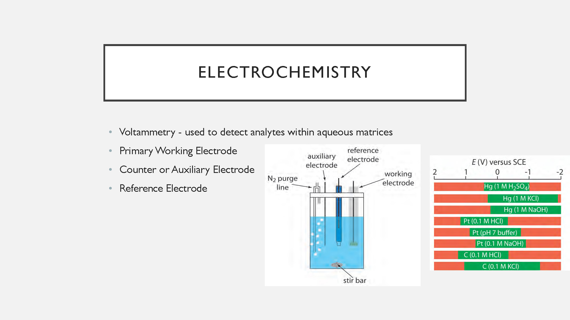
ELECTROCHEMISTRY
- Voltammetry - used to detect analytes within aqueous matrices
- Primary Working Electrode
- Counter or Auxiliary Electrode
- Reference Electrode
USES
- Used to detect biological respiratory analytes in river, estuarine and marine water column and sedimentary environments
- Can be used for both sediment columns and In-Situ
- Understand the pathways and rates of organic carbon degradation to better understand carbon cycling
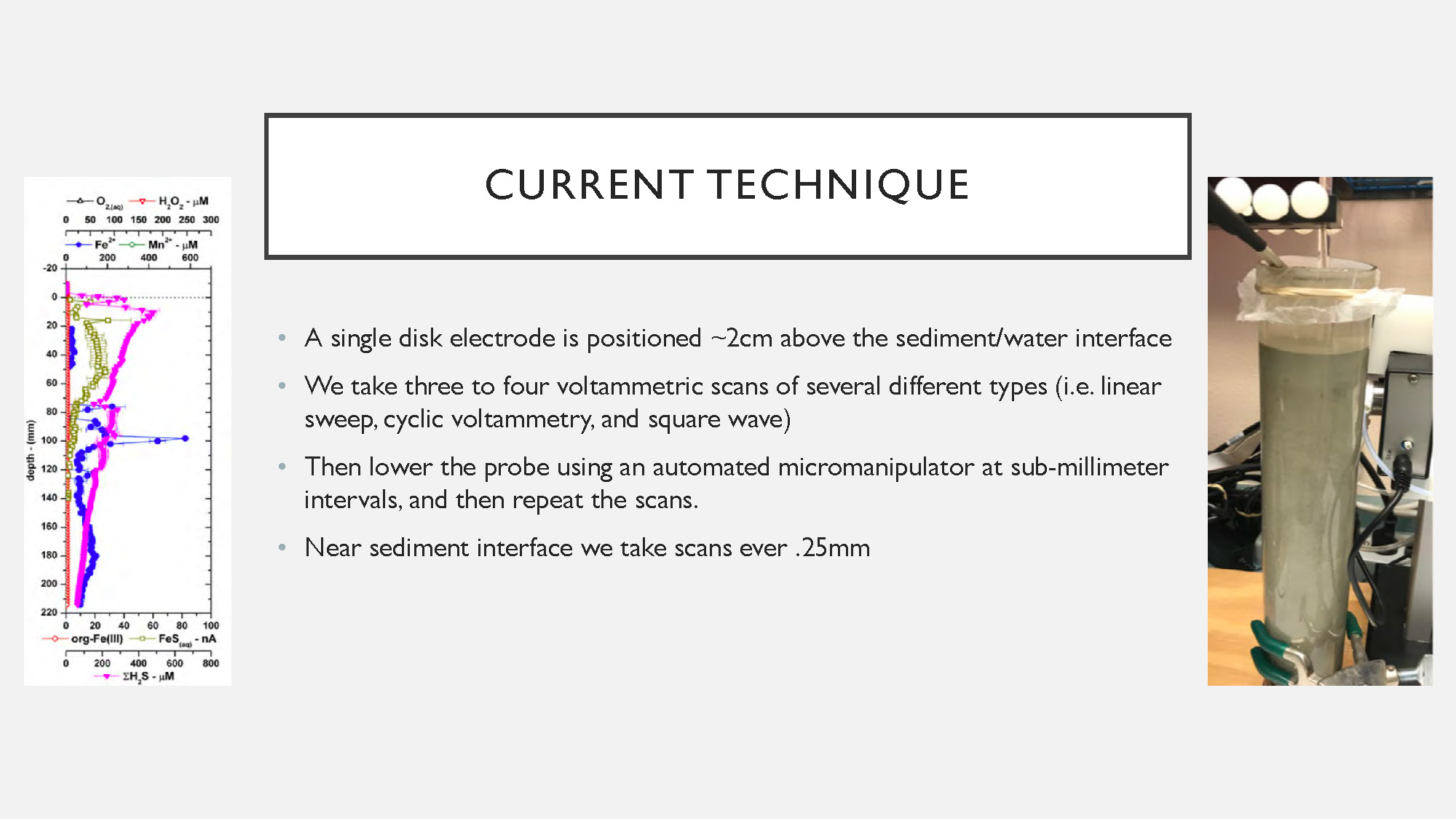
CURRENT TECHNIQUE
- A single disk electrode is positioned ~2cm above the sediment/water interface
- We take three to four voltammetric scans of several different types (i.e. linear sweep, cyclic voltammetry, and square wave)
- Then lower the probe using an automated micromanipulator at sub-millimeter intervals, and then repeat the scans.
- Near sediment interface we take scans ever .25mm
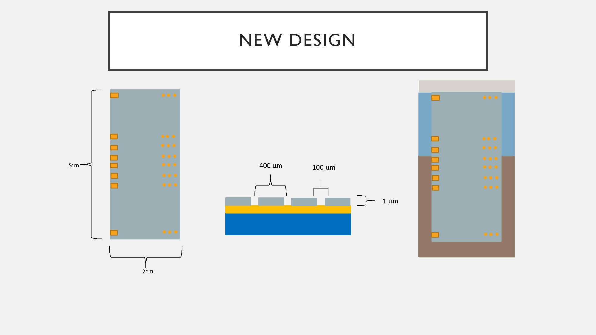
NEW DESIGN
The slide contains three diagrams. The diagram on the left shows a gray, rectangular object that is 5 cm tall and 2 cm wide, with a series of small, orange squares on its surface arranged in two vertical columns. The middle diagram is a cross-sectional view of a multi-layered structure with dimensions labeled: a 1 µm layer, a 100 µm width, and a 400 µm width. The layer on top is gray, the middle layer is blue, and the bottom layer is yellow. The diagram on the right shows a gray, rectangular object, similar to the one on the left, but partially embedded in a brown, uneven surface.
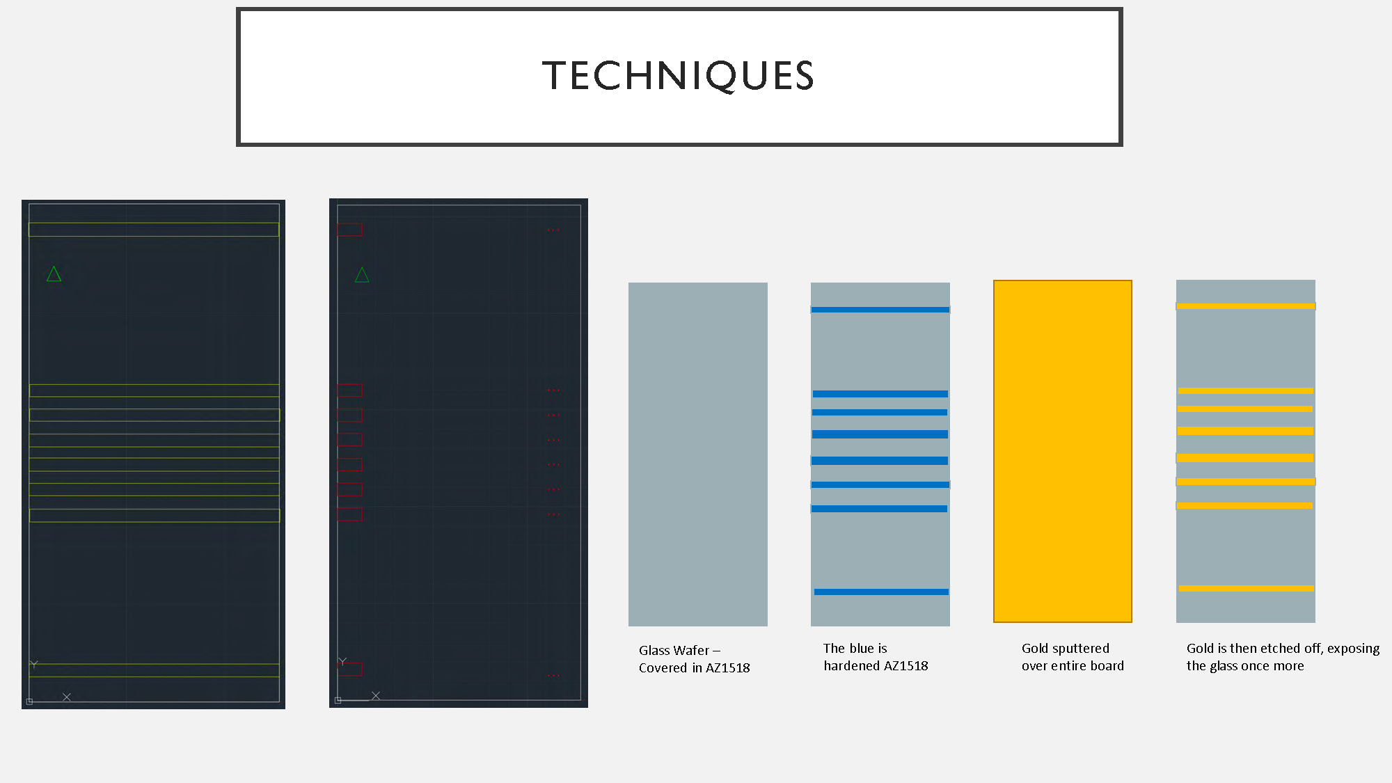
TECHNIQUES
Microfabrication process steps:
Six diagrams arranged in two rows. The top row has two identical diagrams showing a dark gray background with a series of parallel yellow lines. The second row has four diagrams. From left to right, the first shows a gray rectangle labeled "Glass Wafer - Covered in AZ1518". The second shows the same gray rectangle with several blue horizontal lines, labeled "The blue is hardened AZ1518". The third shows a solid yellow rectangle labeled "Gold sputtered over entire board". The fourth shows the same gray rectangle with several horizontal yellow lines, labeled "Gold is then etched off, exposing the glass once more"
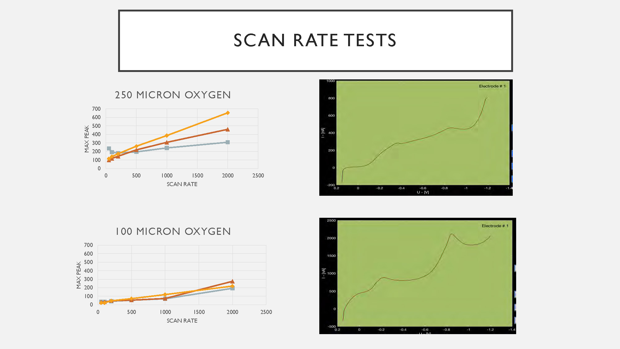
SCAN RATE TESTS
250 MICRON OXYGEN
Graph showing Max Peak (y-axis, 0-700 range) versus Scan Rate (x-axis, 0-2500 range) for 250 micron oxygen electrode testing.
100 MICRON OXYGEN
Graph showing Max Peak (y-axis, 0-700 range) versus Scan Rate (x-axis, 0-2500 range) for 100 micron oxygen electrode testing.
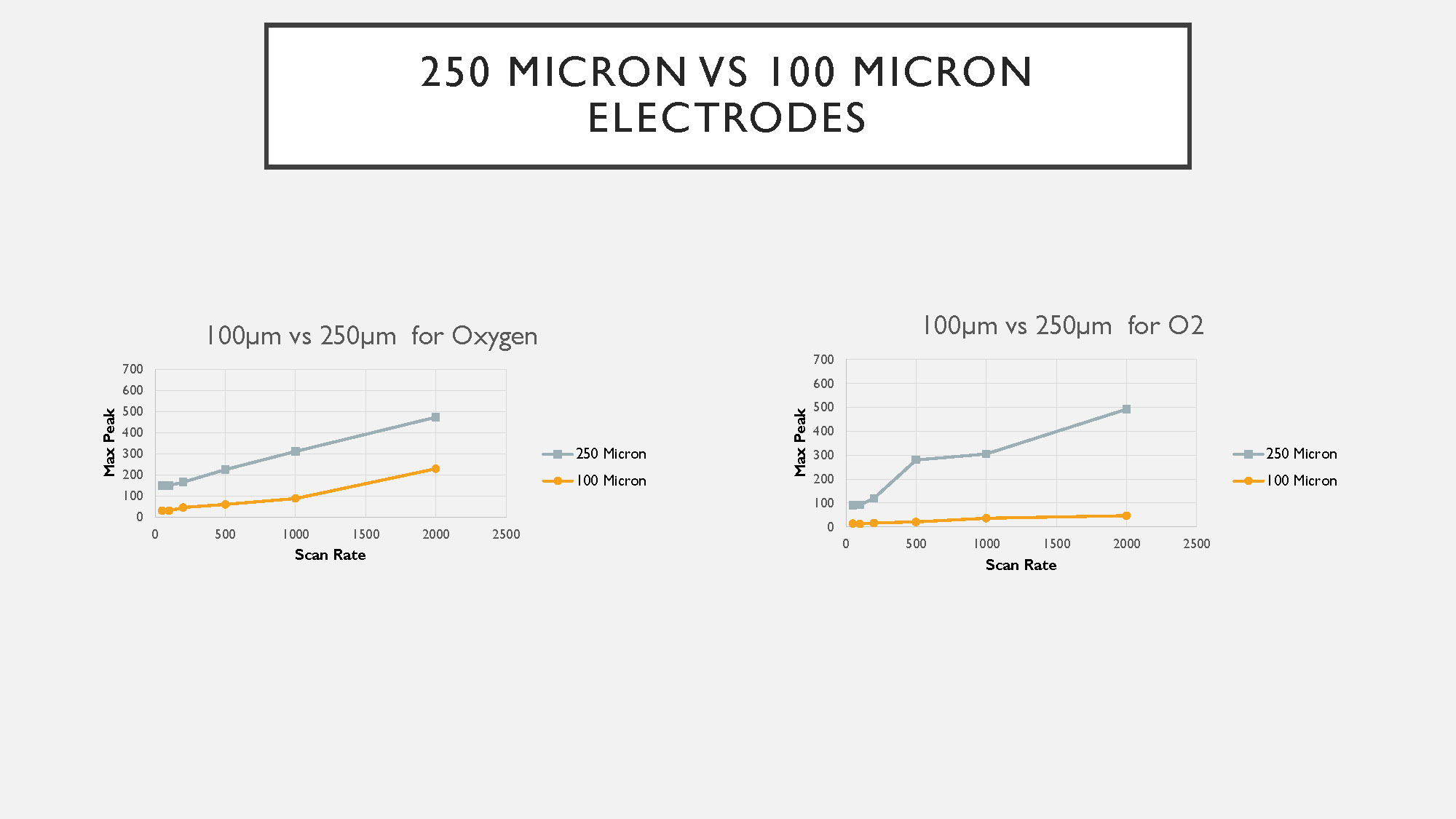
250 MICRON VS 100 MICRON ELECTRODES
100μm vs 250μm for Oxygen
Comparative graph showing Max Peak (y-axis, 0-700 range) versus Scan Rate (x-axis, 0-2500 range) with two data series:
- 250 Micron
- 100 Micron
100μm vs 250μm for O2
Second comparative graph showing Max Peak (y-axis, 0-700 range) versus Scan Rate (x-axis, 0-2500 range) with two data series:
- 250 Micron
- 100 Micron
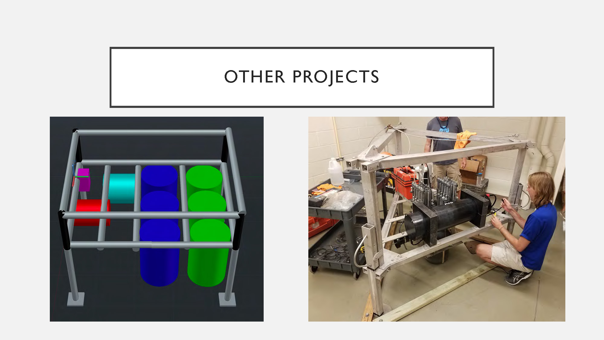
OTHER PROJECTS
The image on the left is a 3D rendering of a gray metal frame holding several cylindrical objects in red, magenta, cyan, and two shades of green. The image on the right is a photograph of two people working on a large piece of equipment made of silver-colored metal tubing and a black, rectangular box. One person is kneeling and appears to be working on wires, while another person is standing behind them.

End of Presentation
Click the right arrow to return to the beginning of the slide show.
For a downloadable version of this presentation, email: I-SENSE@FAU.